Code Protection is a feature offered by microcontrollers to disable storage readout. A developer would typically enable it before the programmed chip lands on customer hands; in principle, disabling code protection would require full erasure of the stored firmware.
Typically, code protection state is stored as a bit in on-board storage, in a dedicated area that can be programmed along with the firmware. The code protection machinery itself is established in bootrom or by a dedicated circuit, or sometimes both.1 The Altera EP900 is an old chip, so it seemed like a reasonable bet that it wasn’t doing anything particularly complex for code protection.
In order to store that bit (or any bit on EEPROM), electrons are contained in a floating gate electrically isolated by silicon dioxide layers. When UV light is applied, it provides enough energy to knock the electrons off the floating gate past the insulating layer, causing them to escape from the floating gate, thus erasing the stored charge and flipping the bit. This is certainly a concern for protecting read-protection bits from further modification.
Read-protect bit erase attempts are mitigated by placing metal shields over (E)EPROM cells, sometimes even by introducing
security meshes
over the silicon and light-sensitive fuses underneath the meshes. The logic can be further complicated by storing read-protect bits dispersed throughout the die and inverting the logic such that charged cells indicate a protected state instead of an unprotected state.
For chips with a large feature size, it’s feasible to control the bit erasure by carefully masking areas of the die and shining UV light at it. On modern chips the distances between EEPROM cells are typically too small to work with using a UV lamp and nail polish; in such cases, other sources of energy may be considered, such as: applying current with a microprobe, shining a narrow-beam laser,2 or shooting particles at it using a Scanning Electron Microscope or a Focused Ion Beam.34
I first learned about the UV read-protect erasure technique through
Bunnie’s blog
, in which Bunnie uses UV to clear the read-protect bit of a PIC 18F1320. He uses masking tape to cover the EEPROM regions and also describes how to clear shielded read-protect bits by shining UV light at an angle to the die.5 Some of the UV light reflects off the bottom of the die towards the top of the shield, which then gets reflected to the memory cell to clears the read-protect bit.
John McMaster let me use his equipment, materials and lab space to perform this research on the Altera EP900, mentored and taught me some of his tricks.6 With all these resources, I performed a similar attack on the Altera EP900.
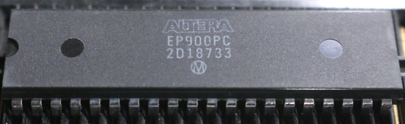
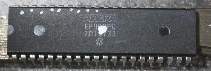
Altera EP900
The Altera EP900 was manufactured in 1985.7 According to the datasheets, both offer a read-protect bit to restrict reading out a programmed bitstream.8
Altera EP900PC Package
Technique sequence
Flash a test pattern
Live-decap the chip with WFNA
Test and identify possible areas on the die related to code protection with nail polish and UV
Cover half of the EEPROM cells in a divide-and-conquer fashion
If code protection is still enabled, the read-protect bit is probably under the nail polish: wipe the nail polish off with acetone, cover the other half and try again
If a partial readout is achieved, the read-protect bit is located in one of the exposed areas: cover half of that exposed area, reflash and try again.
If a full readout is achieved, you’ve identified the location of the read-protect bit!
Flash a test pattern
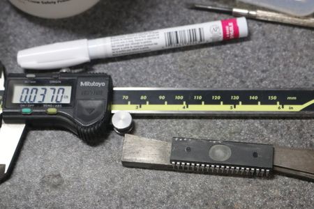
The first step is to generate a test pattern. I’m dealing with a PLD – A pattern of all 1’s would likely cause a latch-up of the PLD circuitry. Latch-up happens when a positive feedback transistor configuration is programmed, leading to VCC and ground short and damaging the sample. Oops!
Instead I generated a test pattern with randomized bits (say, 1s that are four or more bits apart) throughout the programmable region. With the test pattern loaded in, the programmer reports a checksum of 0x2ED3 before applying code protection. After applying code protection, the programmer reads the bitstream as all 1’s and reports a checksum of 0x7684.
The EP900 is meant to be electrically erasable, and I only had epoxy samples, so it was necessary to remove the epoxy packaging to expose the die. It was also necessary to keep the chip in a functional state afterwards. I decapped the epoxy packaging with heated WFNA (White Fuming Nitric Acid, a highly concentrated HNO3 solution) in order to utilize UV erasure.
Live-decap with WFNA
The EP900 has gold bond wires, which don’t oxidize under WFNA exposure. In the case of copper bond wires a mixture of
HNO3 : H2SO4
is recommended.
Before depositing WFNA on the sample, mill out an oval depression over the center of the package, over the area of the die (usually in the center). This will reduce the amount of WFNA required to expose the die and mitigates and reduces the amount of dissolved carbon sticking to the die (rendering parts of it opaque).
There are some guides on acid decapsulation, some of them referred to in the
decapping references
section.
Here is my process for this particular target:
Mark the center of the package in preparation for milling. The suggested depression depth range for a PDIP40 is
0.035″ - 0.040″ (0.89 mm - 1.01 mm)
.
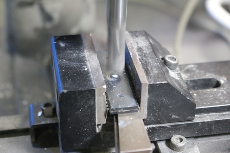
Center mark for the EP900
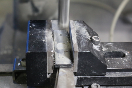
Place the package snug on an adjustable parallel, and place it on a mount for milling. Mark the package with the endmill to make sure it’s centered with the center marking.
Verifying that the endmill is centered
Carefully mill the depression. Once you get the required depth, move the sample back and forth to get an oval depression.
Partial milling of the epoxy packaging
Measure the depression depth from its center with calipers. If the measurement falls within the depth target described above, the sample is likely ready to be placed on the hotplate. You might have to experiment. If there are indications of bond wires or the die (shiny features in the epoxy), you may have milled too far and a new sample should be milled with an adjusted depth.
Target depth achieved
Set the hotplate to 200 F - 215 F (90 C - 100 C) and place the sample on it. Once heated, use a pipette to place 2 - 3 drops of WFNA in the depression. Wait until it starts bubbling (10 to 20 seconds), then remove the sample and spray it with acetone to remove the reaction products.
Bubbling WFNA at 200 F
After the acetone dries off, visually inspect the decap. In this case, the bond wires are exposed by the WFNA after the first round.
Partial decap (first round)
Repeat steps 5 and 6 until the die is fully and cleanly exposed. In this case, a four rounds were required to remove the epoxy residue from the die.
Partial decap (third round)
Once it looks clean, inspect the die and bond wires under an inspection microscope for any potential damage and attempt to read an ID code from the sample with a programmer.
Handling white fuming nitric acid requires considerable precaution. Fuming HNO3 reacts exothermically with water and especially acetone, requiring special care when neutralizing it and storing it in waste containers. WFNA, in particular, will react exothermically with latex and nitrile gloves. Breathing the fumes in can be particularly unhealthy, and skin contact will result in burns.
I used a fumehood to isolate the fumes, a respirator for extra precaution, a long-sleeve labcoat, latex gloves (NOT A GREAT IDEA but it gave me about five seconds to remove them if they come into contact with a drop of WFNA), and baking soda to neutralize any spills.
Integrated Circuit Failure Analysis: A Guide to Preparation Techniques, Friedrick Beck, Chapter 2.3
Identify EEPROM
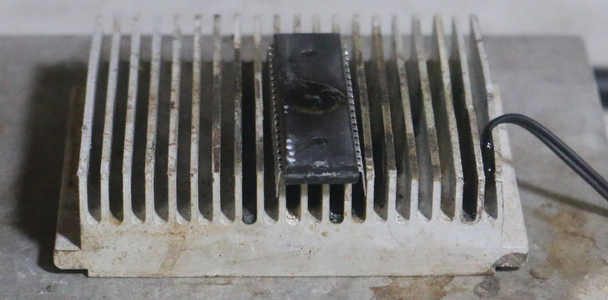
With the target decapped, I verified that the sample is still operational and is erasable via UV. I also verified that the read-protect bit is erasable under UV applied perpendicular to the die. As discussed in Bunnie’s experiment, the read-protect bit can be covered with a metal shield, which might require placing the target at an angle with the UV light source. The EP900 does not have such a shield. Since there is no shield, I had to seek it out through trial and error.
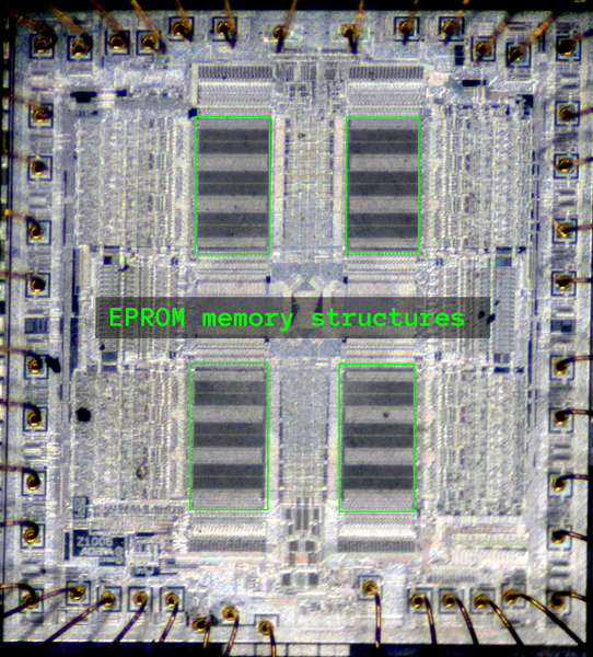
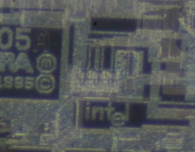
There are four large memory storage structures, as viewed under an inspection microscope, indicated by the rectangleness and regularity of their shape. The datasheet does not indicate the presence of SRAM on the die, so it’s likely that all four of the memory structures are EEPROM.9
EP900 die with EEPROM regions marked
Masking EEPROM and identifying the read-protect bit cell
(The masking process in another article I wrote but haven’t published here yet
masking EEPROM on an 8752
. Hence, in one of the pictures is a different chip – same principle, though).
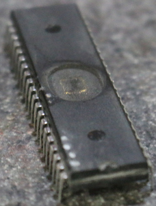
I used nail polish to cover features of the die from UV light (my mask). I isolate the read-protect bit by bisecting the silicon area after each test, eventually narrowing down on its position.
It’s good to test if the read-protect bit is stored in the EEPROM region in the first place. To start, cover all the EEPROM regions and check if UV light clears the read-protect bit; if it does, then the read-protect bit is stored somewhere else on the die. In this case, the test confirmed that the read-protect bit is stored in the EEPROM regions.
Cover half of all the EEPROM cells and test it for read-protect bit erasure. If applying UV erased the read-protect bit, reprogram the chip with the same pattern and then mask half of the unmasked region (covering 3/4th of the EEPROM space). Repeat this process until fewer and fewer bits are erased in the EEPROM. If the read-protect bit is stored on the edge of the EEPROM, then this process works rather quickly.
Mask application setup for the Intel 8752
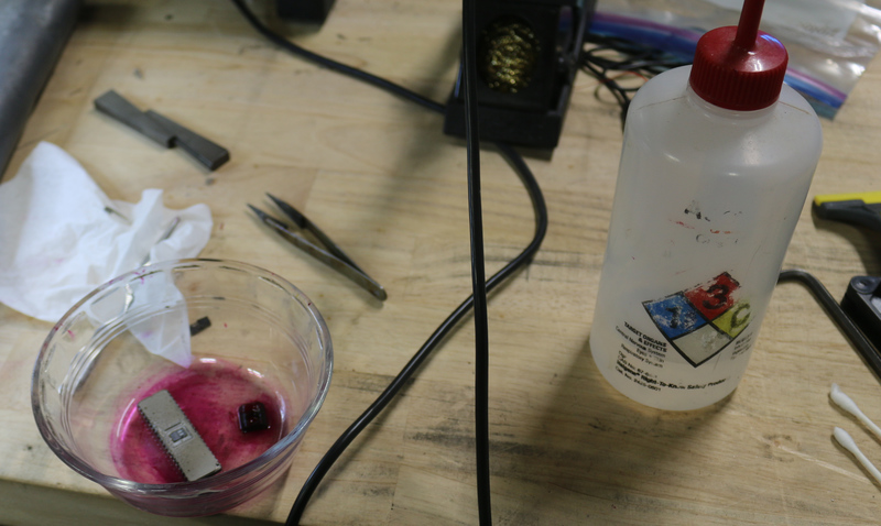
To apply the nail polish, I placed the chip in a bowl filled with a small amount of acetone. The acetone vapors delays the nail polish from drying, making it more fluid when applied to the die region.
It was necessary to experiment to find the right amount of acetone for this setup. Too much acetone made the nail polish too fluid and difficult to contain. The acetone gives the nail polish more of the watercolor consistency. The acetone pool can also be used for cleaning off the brush.
It was also necessary to use a very thin brush to apply the nail polish. I used a strand of my own neckbeard hair as the brush.
My process for applying the nail polish mask:
Place the chip and a small block in a small bowl. The block will be used as a nail polish pallet, to avoid removing the brush from the bowl and drying it out.
Pour a little bit of acetone into the bowl. The exact amount requires experimentation.
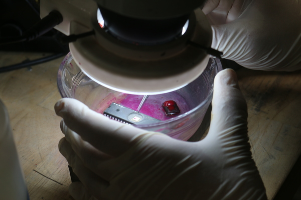
Place the bowl under an inspection microscope and set the focus on the die.
Put some nail polish on the pallet.
Take a brush (like a strand of hair), dip it in the nail polish pallet. After this point, do not remove the brush from the bowl until you’re done applying the nail polish.
Proceed to apply nail polish to the EEPROM region until it’s fully covered. It is probably OK to cover the row decoders surrounding the EEPROM memory arrays.
Once you have your region covered, remove the chip from the bowl to dry the nail polish deposited on the die. Clean the brush with acetone and remove it from the bowl.
To redo the process, spray acetone on the die until all the nail polish is removed. Make sure not to spray it too hard as it increases the risk of breaking the bond wires.
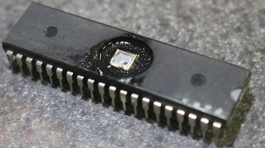
Applying nail polish to the EEPROM regions of the EP900 die
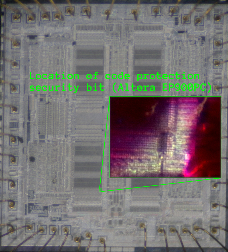
After some rounds of this, I found that leaving the bottom-left EEPROM structure uncovered under UV clears the read-protect bit. To verify the location of the read-protect bit, I masked the entire die except for one of the corners, to test the hypothesis that the read-protect bit would be stored in the first or last row and column of the memory structure.
After:
reprogramming the test pattern
setting the read-protect bit
leaving the bottom-right of the EEPROM structure unexposed
and clearing the read-protect bit with UV
A readout of the EP900 yields a matching checksum (0x2ED3) to the test pattern. Success!
Nail polish surrounding the read-protect bit region
Results
I got somewhat precise information about where the read-protect bit is for the EP900. Had it been possible to use a test pattern filled with 1s, it could have been possible to match the memory-space to the geometry of the EEPROM rows and further optimize the search algorithm.
It is worth noting that the read-protect bit is stored at a corner of the EEPROM bank. There’s a heuristic here: configuration bits would likely be stored at an edge or corner of a EEPROM bank, instead of alongside data and code memory, because the structure is designed by a human with human tendencies. From an engineering standpoint the placement is intuitive, because we make physical structures that map to the abstractions we use to implement them, so that their structures are analogous to each other. It’s a memetic aid, but as you can see leads to predictable blindspots.
Acknowledgements
Thank you
John McMaster
for letting me visit his homelab again, where you lent me your equipment and expertise while working on this project. Cheer bro!
When bootrom is involved for checking code protection, it may be able to do other things such as to check for passwords before establishing an in-circuit debugging session via JTAG, and auto-wipe the firmware if too many incorrect attempts are detected. ↩︎
Many other sources of energy can be considered, the main point is to achieve a desirable level of control over where that energy goes throughout the topology of a chip and the constraints imposed by geometries surrounding the target. ↩︎
Heuristic: high-performance signals processing amplifies the effects of noise, or brings signal-level closer to the noise-level. This seems more evident as modern VLSI raises the ante on moore’s law, feature sizes get closer to Planck’s length and energy-requirements to switch transistors and re-write memory cells decreases. The energy-requirements become so small that neighboring cells and traces couple with each-other, providing each other a source of additional charge from the flux of their surrounding electromagnetic fields. (CORRECTION: electrostatic fields; even though this specific attack is electromagnetic).
Modern FLASH firmware will randomize bits as they are written to cells because the charge field gradients generated by regular geometries in a tight space can be larger and saturated enough to donate electrons to neighboring empty electron wells, effectively flipping its own bits.
ROWHAMMER
exemplifies an attack using the same principle in random-access memory, where neighboring DRAM cells can be made to pulse in geometries that activate previously uncharged neighbors. ↩︎
Note how the presence of the read-protect bit shield reveals the read-protect bit’s position on the silicon, which saves Bunnie time from having to search for it; I think it’s a good example of the castle wall dilemma (or whatever you call it). ↩︎